Single Cycle Processor
Visit Code Repository
Table of Contents
1. Overview
Till now you have learned to design sequential and combinational logic, in this section you will learn how to create a single cycle processor, specifically the MIPS microprocessor.
This section combines almost every concept covered so far. Abstraction of block diagrams and Verilog HDLis used to describe the arrangement of each component. We exploit regularity and modularity by reusing already created blocks such as ALUs, multiplexers and register files. The microarchitecture is partitioned into datapath and control units. The MIPS microprocessor datapath uses the register file, ALU, memory unit, and instruction decoder to execute instructions. The register file stores data and instructions, the ALU performs operations, the memory unit accesses and stores data, and the instruction decoder controls data flow. The control unit of a MIPS microprocessor generates control signals that direct the flow of data between components in the datapath, ensuring that instructions are executed correctly. It receives instructions from the decoder, directs data flow to the correct components, and controls instruction timing.
Together, the datapath and control units work to execute instructions in the MIPS microprocessor.
We will focus on the single-cycle implementation of a subset of MIPS instructions. Additionally, we will compare single-cycle, multicycle, and pipelined microarchitectures for the MIPS processor.
2. Prerequisites
To create a Verilog MIPS single cycle processor, you should have a strong understanding of digital logic design, computer architecture, and Verilog programming.
Some of the specific prerequisites include-
Knowledge of digital logic design concepts, such as combinational and sequential circuits, logic gates, flip-flops, and registers and implementing these in Verilog HDL.
Understanding of computer architecture principles, including datapath and control unit design, memory organisation, instruction decoding, and input/output interfaces. These are also covered once more in the “Theory” section of our module.
Experience with Verilog programming, including the ability to write and understand Verilog code, testbenches, and simulation results.
Ability to use simulation and synthesis tools, such as ModelSim, Quartus, to simulate and synthesise Verilog code.
Knowledge of computer organisation and assembly language programming is also beneficial, as it provides context for understanding the MIPS single cycle processor and its operation.
Additionally, it would be helpful if you were familiar with the MIPS instruction set architecture, including its various instruction formats, opcode values, and functionality.
3. Control Unit
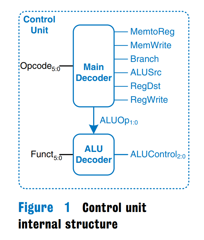
This section covers an implementation of our MIPS subset, which is created by adding a basic control function to the datapath discussed in the previous section. Support for load word (lw), store word (sw), branch equal (beq), and arithmetic-logical instructions like add, sub, AND, OR, and set on less than are all included in this version. It is implemented in 2 parts: the main control Unit and ALU Control Unit. Firstly we look at the instruction format.
Instruction Format
The 32 bit MIPS instruction can be broken down into the following parts

fig 2
The op field, called the opcode, is always contained in bits 31:26. We will refer to this field as Op[5:0] by standard notation.
The two registers to be read are always specified by the rs and rt fields, at positions
25:21and20:16. This is true for the R-type instructions, branch equal, and store.The base register for load and store instructions is always in bit positions
25:21(rs).The 16-bit offset for branch equal, load, and store is always in positions
15:0.The destination register is in one of two places. For a load, it is in bit positions 20:16 (rt), while for an R-type instruction it is in bit positions 15:11 (rd). Thus, we will need to add a multiplexor to select which field of the instruction is used to indicate the register number to be written.
Main Control Unit (Main Decoder)
The control unit computes the control ignals based on the opcode and funct fields of the instruction, [31:26] and [5:0].
Most of the control information comes from the opcode, but R-type instructions also use the funct field to determine the ALU operation. The majority of the outputs from the opcode are computed by the main decoder. The 6 bits of the opcode are decoded into various control signals of the Main Decoder as shown in Fig. 3.
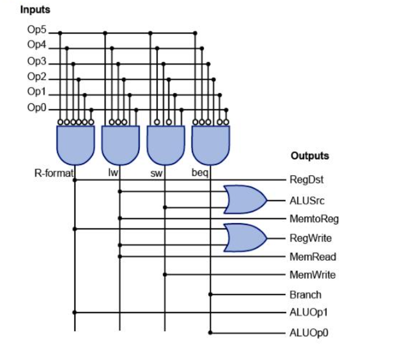
Fig 3. Simple PLA Implementation
Table 1 explains each of the control signals in detail with all the important information. These nine control (two from ALUOp which are explained later) signals are set on the basis of six input signals to the control unit, which are the opcode bits 31 to 26.
| Control Signals | Deasserted | Asserted |
|---|---|---|
| RegDst | The write register number comes from the rt field (20:16) | The write register number comes from the rd field (15:11) |
| RegWrite | - | The register on the write register input is written with the value of the Write data input. |
| ALUSrc | Second ALU Operand is the second register file output. | Second ALU Operand is the sign extended offset (16 bit to 32 bits) |
| PCSrc | PC = PC + 4 (For sequential exec.) | PC is replaced by branch target. |
| MemRead | - | Data memory contents designated by address input are put in Read Data Output. |
| MemWrite | - | Data memory contents designated by address input are put in Write Data Output. |
| MemtoReg | Write Data is fed input from ALU. | Write Data is fed input from Data Memory. |
Table 1. Different Control Signals for the different MUXs
With the exception of the PCSrc control line, the control unit can set all of the control signals based only on the opcode field of the instruction. If the instruction is branch on equal and the ALU's Zero output is asserted, then the PCSrc control line should also be asserted. We must AND the Zero signal from the ALU with the Branch signal from the control unit in order to produce the PCSrc signal.
ALU Control Unit (ALU Decoder)
Depending on the instruction class, the ALU will need to perform one of these functions.
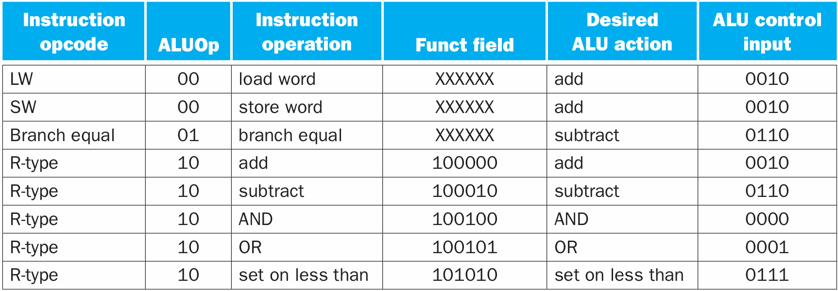 Table 2. ALU Control Lines
The main decoder determines a 2-bit ALUOp signal which is used as input for ALU Decoder along with the 6-bit funct (or function) field in the low-order bits of the instruction. The 4 bit output signal of the ALU Control Unit represents the operation to be carried out by the ALU. 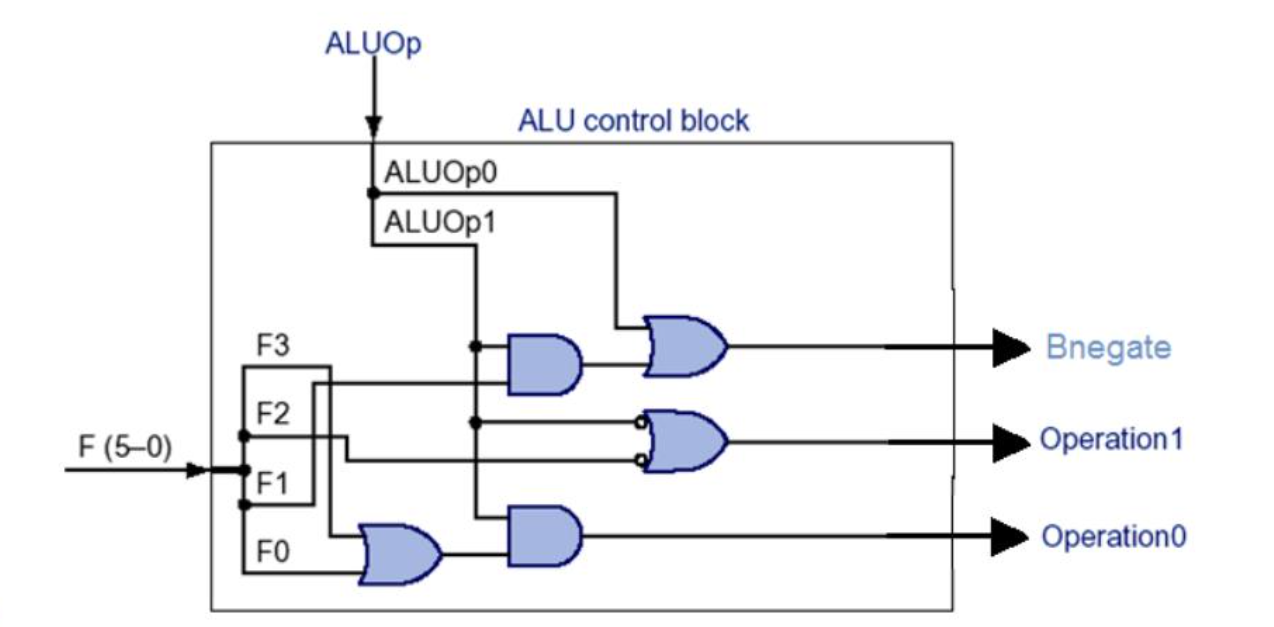 Fig 4. ALU Hardware Implementation
The 2 bit ALUOp sent by the Control Unit indicates whether the operation to be performed should be add (00) for loads and stores, subtract (01) for beq, or determined by the operation encoded in the funct field (10).
Understanding the optimal implementation:
Using multiple levels of control can reduce the size of the main control unit. Using several smaller control units may also potentially increase the speed of the control unit. Such optimizations are important, since the speed of the control unit is often critical to clock cycle time
ALU Control Truth Table

Input-Output Truth Table
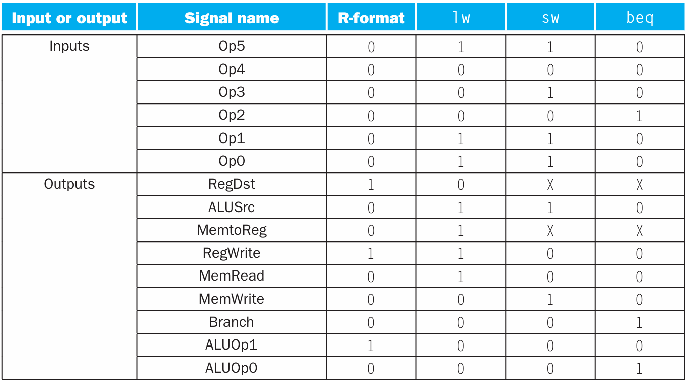
4. Datapath
A datapath is the part of a computer processor that performs arithmetic and logic operations on data. It is a digital circuit that consists of registers, an arithmetic logic unit (ALU), and multiplexers.
The datapath receives instructions and data from the processor's memory and performs the necessary operations specified by the instructions. The ALU performs arithmetic and logical operations on the data, and the registers store intermediate and final results.
The datapath also includes multiplexers that allow the selection of different input values based on control signals. The control signals are generated by the control unit, which coordinates the operations of the datapath to execute instructions.
The datapath operates on words of data. MIPS is a 32-bit architecture, so we will use a 32-bit datapath. The datapath first decodes the instruction for the control unit which then sets the different multiplexers thereby fixing the datapath. We will split the datapath into different state elements and try to learn them one by one and finally piece them together to create a complete datapath.
State elements
There are 5 main state elements required for building the datapath.
a Instruction Memory
The program counter contains the address of the instruction to be executed. The first step is to read this instruction from the element called instruction memory. The instruction memory takes the address in PC as the input and fetches the 32 bit instruction, labelled instr.
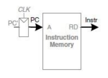
The processor’s actions depend on the specific instruction that was fetched.
b Register File
The register file contains all the available registers. It has two read ports and one write port. Since MIPS architecture contains 32 registers, each register is identified by a unique 5 bit number (log2 32). This unique 5 bit number is given as the input in both read and write ports. The contents of the registers specified via the read ports are given as the output. If the control signal RegWrite is set, the data given in the data port is written into the register given in the write port.
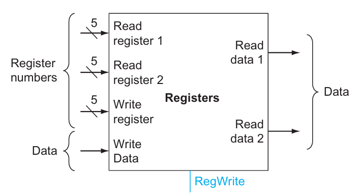
c) ALU
ALU performs different arithmetic operations on the data depending on the signal received from the control unit. It has two data input ports and an input from the control unit which specifies the operation to be performed. The final result is output through ALU result and zero port is set to 1 if the result is zero.
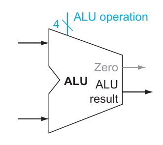
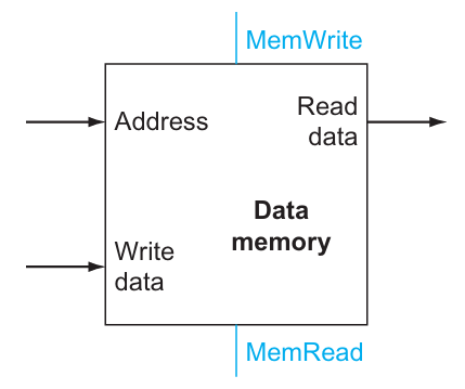
d Data Memory
The memory unit is a state element with inputs for the address and the write data, and a single output for the read result.There are separate read and write controls, called MemRead and MemWrite. Only one of these may be asserted at a time.
- If
MemReadis set then value at the address given is fetched and outputted through the read data port. - If
MemWriteis set then the value at the address is changed to write data.
e) Sign extension
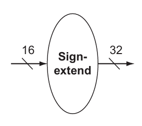
To understand what sign extension is, let’s take an example. Consider the 4 bit number 1100. If we were to sign extend it to an 8 bit number, we take the MSB which in this case is 1 and extend it to make the upper half of the 8 bit number keeping the lower same as the initial 4 bits which gives us 1111 1100. Similarly, this element sign extends a 16 bit number into a 32 bit number.
Now that we have seen the different state elements involved in a datapath, let's see the datapath followed by different MIPS instructions. Since we are considering MIPS microprocessor, each instruction is 32 bits long.
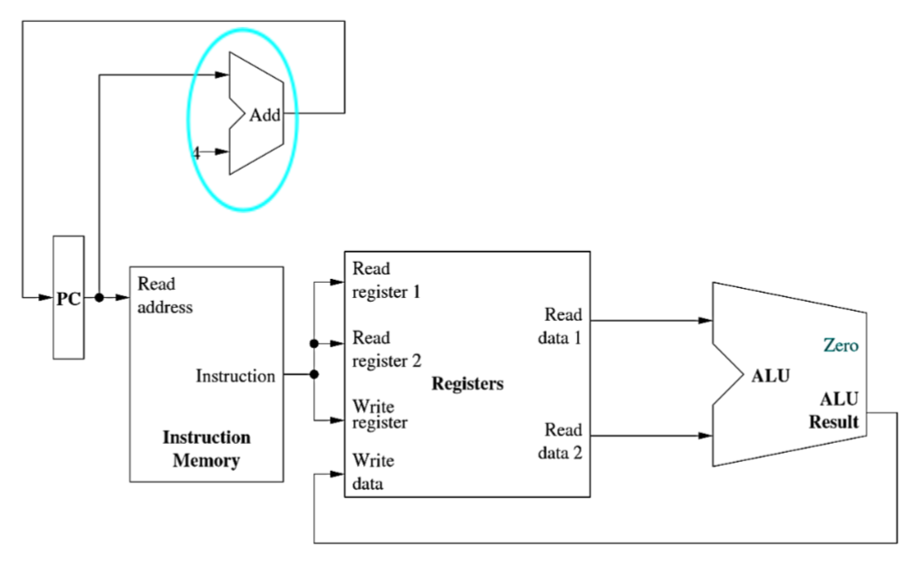
- add It is an R-type instruction of the form add $rd,$rs,$rt The R-type instruction format is

The datapath for add instruction is as follows :
- Grab the instruction address from the PC.
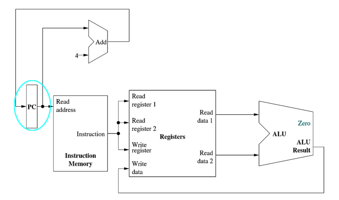
- Decode instruction.
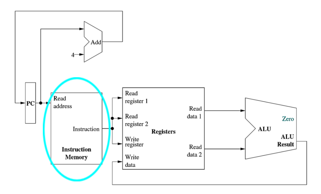
- Pass rs,rt and rd into read register and write register ports.
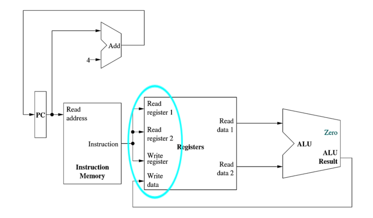
- Retrieve data from read register 1 and register 2 (rs and rt).
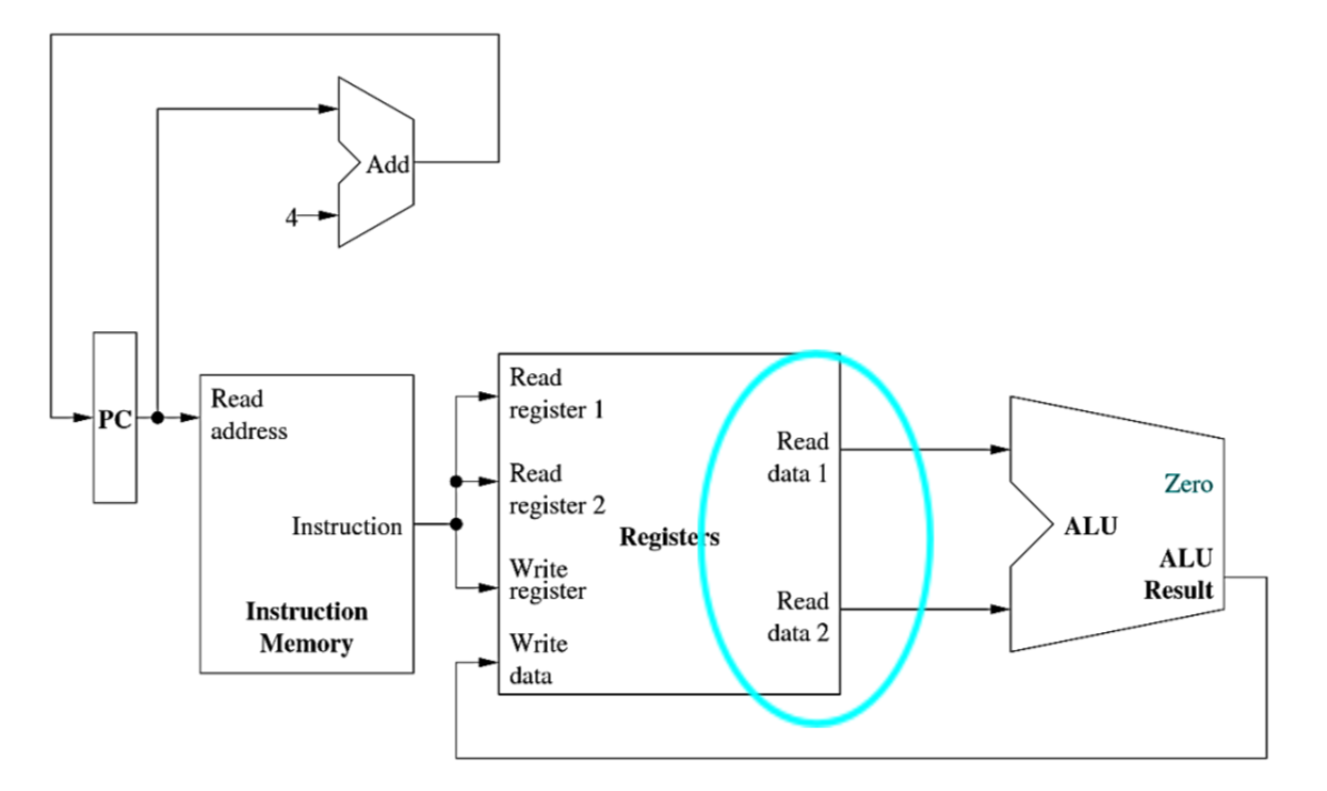
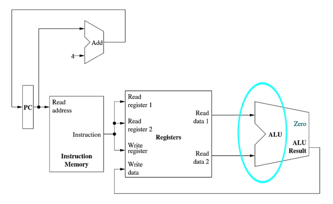
- Pass contents of rs and rt into the ALU as operands for the addition operation. The only difference between different arithmetic operations is in the ALU operation performed.
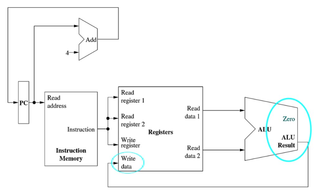
- Return back the ALU result to the register file as the Write data argument. The data will be written into the Write register specified by the rd field.
- Increment the value of PC to PC+4 to move on to the next instruction.
lw(load word)
The lw instruction is of the formlw $rt immediate($rs). It has an I-type instruction format.

The load word instruction copies the data stored at the address ‘immediate+value(rs)’ and stores it into the register rt.
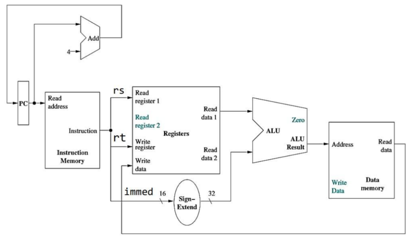
The datapath for lw instruction is as follows :-
The instruction memory reads the PC and outputs the instruction.
The control unit examines the most significant five bits of the instruction to determine the necessary datapath configuration.
The register file receives the two register numbers rs and rt, with rs connected to the read port and rt to the write port. Read data 1 port outputs the data stored in rs.
This output is then added to the sign-extended immediate using ALU.
The ALU result is sent to the data memory unit, which reads the data stored at the address specified by the ALU result.
Finally, the data read from the memory is returned to the register file, which writes it into register rt.
PC is incremented to PC+4.
sw(store word)sw instruction is of the formvsw $rt immediate($rs)The instruction format is again of the form I-type with an opcode 43.
The store word instruction writes the data stored in the register rt into the memory address ‘value(rs)+immediate ’.
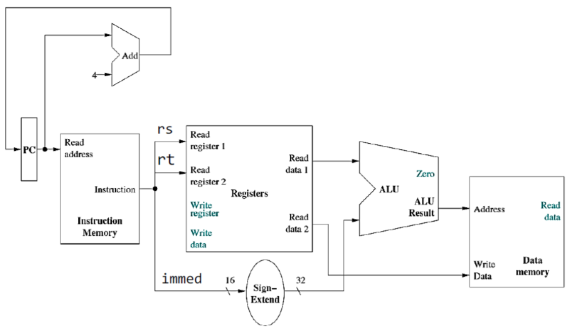
The datapath for sw instruction is as follows :-
The instruction memory reads the PC and outputs the instruction.
Control unit examines the most significant five bits and determines the necessary datapath configuration by setting the multiplexers.
The register file receives two register numbers rs and rt, with rs connected to read port1 and rt connected to read port2. The data stored in registers rs and rt is output through the read data port1 and read data port2 respectively.
The read data1 is then added to the sign-extended immediate using ALU.
The ALU result along with read data2 (which contains the value stored in register rt) is sent to the data memory unit, which writes the read data2 into the address specified by the ALU result.
PC is incremented to PC+4.
beq(branch if equal)
The beq instruction is of the form
beq $rs ,$rt ,immediateIt has an I-type instruction format.

It compares the contents of rs and rt to check if they are equal and uses the 16-bit immediate field to compute the target address of the branch relative to the current address.
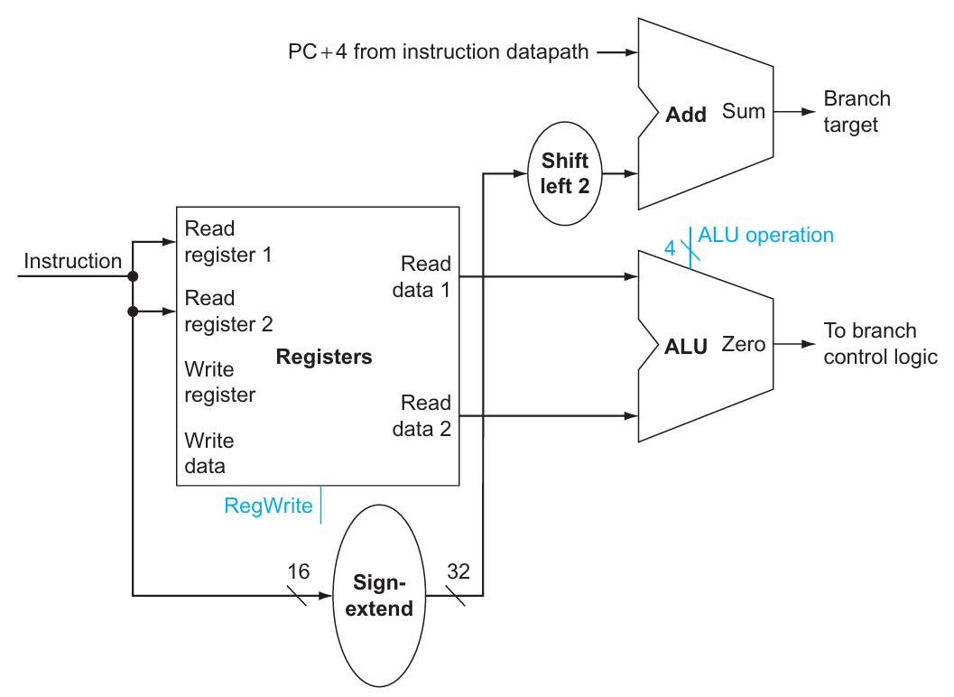
The datapath for beq instruction is as follows :-
The instruction memory reads the PC and outputs the instruction.
Control unit examines the most significant five its and determines the necessary datapath configuration.
The register file receives two register numbers rs and rt in the read register port and outputs the contents in rs and rt.
ALU subtracts the value of rs from rt and sets the zero port to 1 if the result is 0.
The immediate value is sign extended and then shifted left by 2 bits.
PC is incremented to PC+4 and is added with the immediate value to give the branch target.
PC is changed to the branch target if zero port was set to 1.
j(jump)
The jump instruction is of the form j targaddr. It has a J-type instruction format with opcode 2.
This instruction uses the 26 bit targaddr to compute jump address and updates the value of PC to jump address.

The datapath for j instruction is as follows :-
The instruction memory reads the PC and outputs the instruction.
Control unit examines the most significant five bits and determines the necessary datapath configuration.
The 26 bit targaddr is shifted left by 2 bits to create a 28 bit result
Concatenate the result with the upper 4 bits of PC+4 to get the jump address.
Finally, the PC gets updated to the jump address.
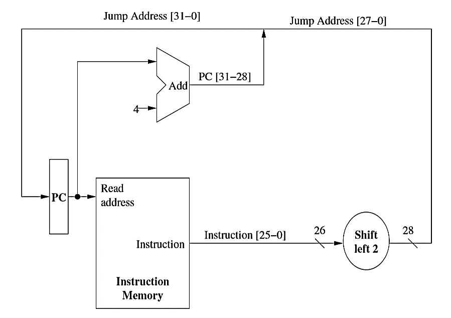
The Final Datapath
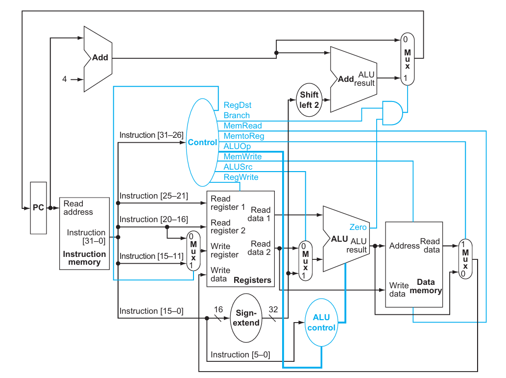
Fig 4. Simple datapath with control unit (for R-type and I-type)
Here, the input to the control unit is the 6-bit opcode field from the instruction. The outputs are the control signals which serve various purposes :-
RegDst,ALUSrc,MemtoReg- 1-bit signals that control the multiplexors.RegWrite,MemRead,MemWrite- Signals that control reads and writes in the data memory and register file.Branch- Signal used in checking if a branch is required.ALUOp- 2-bit control signal for the ALU.
Note that here, the AND gate is used to combine the Branch control signal with the Zero output from the ALU. This is responsible for the selection of the next PC.
Role of Multiplexors
As seen above, there are 4 multiplexors required at various stages of the datapath. They are needed in order to implement both R-type and I-type instructions using the same datapath. Their roles are explained below :-
MUX 1 - This MUX determines which register needs to be written into using the
RegDstcontrol signal. If it’s 0, the write register number comes from the rt field (in the case of I-type), whereas if it’s 1, the write register number comes from the rd field (for R-type instructions)MUX 2 - This MUX is placed at the ALU input with
ALUSrcas the select line. When it’s 0, an arithmetic-logical instruction is taking place, and the second ALU operand is the data read from the second register. When it’s 1, a memory instruction is taking place, with the second ALU operand being the sign-extended 16-bit immediate field from instruction.MUX 3 - It chooses which value is stored in the destination register using the
MemtoRegcontrol signal. This value comes from the ALU (for an R-type instruction) or the memory (for a load).MUX 4 - The final MUX is used to select if the PC moves onto the sequentially following instruction address (PC + 4) or branches to a target address. The control signal that achieves this is the output of the
AND gatewhich is 1 in case of a branch instruction and 0 otherwise.
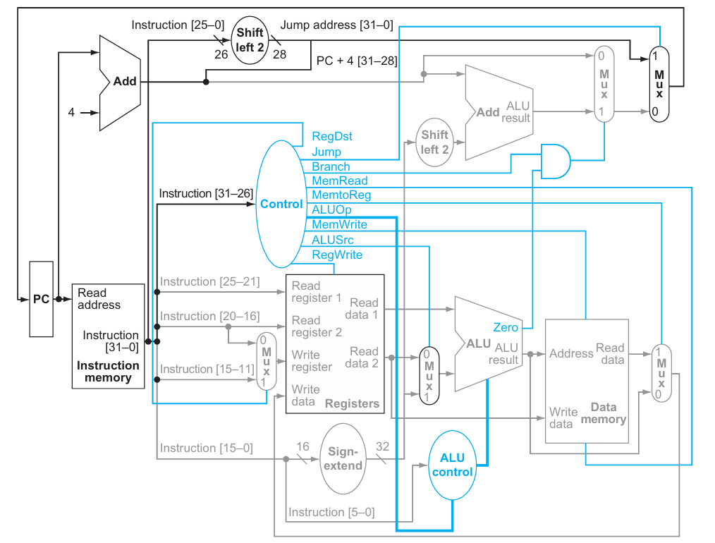
Fig 4. Datapath with Jump implementation
Additionally to implement the Jump instruction in the same datapath, an additional MUX, controlled by the jump control signal, is used to determine whether to move to the jump target address or the next consequent instruction. This jump target is obtained by shifting the lower 26 bits of the jump instruction left 2 bits (ie. multiplying by 4) and then concatenating the upper 4 bits of PC + 4 as the high-order bits, thus yielding a 32-bit address.
5. Implementation
1. Top level module
module top (input clk, reset,
    output [31:0] writedata, dataadr,
    output memwrite);
    wire [31:0] pc, instr, readdata;

    // instantiate processor and memories
    mips mips (clk, reset, pc, instr, memwrite, dataadr, writedata, readdata);
    imem imem (pc[7:2], instr);
    dmem dmem (clk, memwrite, dataadr, writedata,readdata);
endmodule
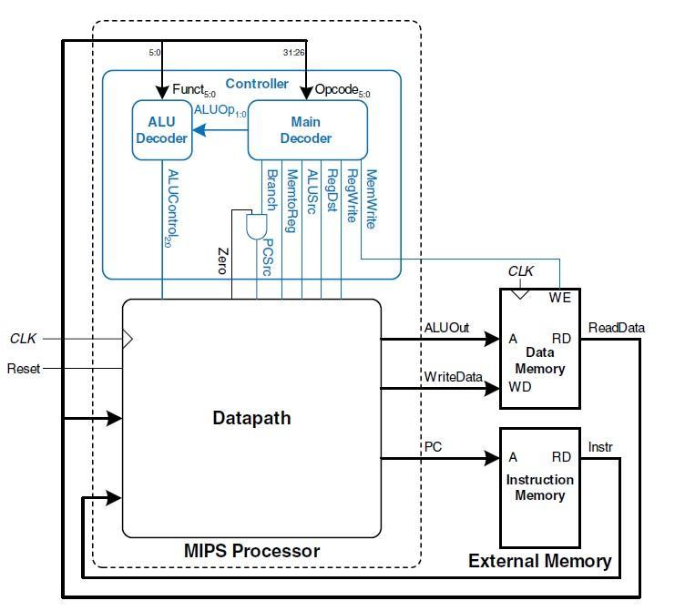
The top level module instantiates 3 sub modules asm , imem and dmem The mips module is the main processor that is responsible for executing instructions. The imem module is the instruction memory, which contains the program instructions. The dmem module is the data memory, which is used for load/store instructions. Here is a brief description of the input and output ports of the top module:
Inputs
clk- the clock signal used to synchronise the processor.reset- the reset signal used to initialise the processor.
Outputs
writedata- the data to be written to memory.dataadr- the memory address to access.memwrite- the control signal for writing to memory.pc- the program counter, which contains the memory address of the current instruction.instr- the current instruction being executed.readdata- the data read from memory.
Overall, the top module provides the infrastructure to execute programs on the MIPS processor. It loads the program instructions from memory, executes them, and stores the results back into memory if necessary.
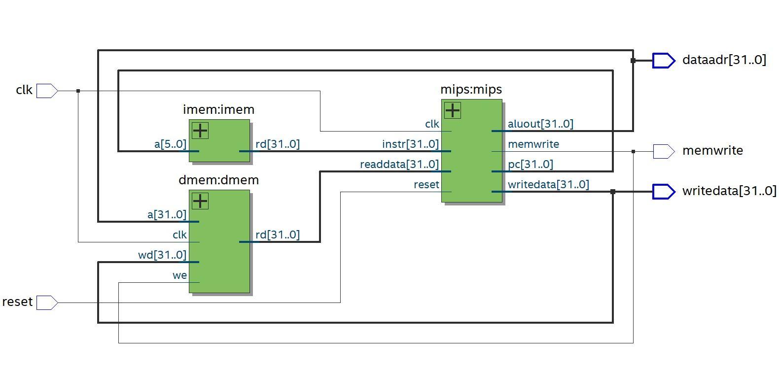
RTL view of top level module
2. Data Memory
module dmem (input clk, we,
            input [31:0] a, wd,
            output [31:0] rd);

    reg [31:0] RAM[63:0];
    assign rd RAM[a[31:2]]; // word aligned
    always @ (posedge clk)
        if (we)
            RAM[a[31:2]] wd;
endmodule
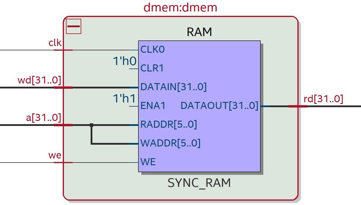
dmem represents a random access memory (RAM) block that can store and retrieve 32-bit data values.
Inputs-
- clk
- MemWrite
we- control signal that determines whether to write data to memory. - 32 bit memory address
a - 32 bit WriteData ‘wd’- data to be written to the location specified by
a.
Output-
- 32 bit ReadData
rd- data read from memory locationa. Thedmemmodule contains a RAM that stores 64 words each of size 32 bits. When theweinput is set to 1, the 32 bit datawdgets written into the memory locationaat the positive edge ofclk.
3. Instruction Memory
module imem (input [5:0] a,output [31:0] rd);
    reg [31:0] RAM[63:0];
    integer i;
    initial
        begin
            $readmemh ("E:\memfile.dat",RAM);
        end
    assign rd = RAM[a]; // word aligned
endmodule
Input :
- 6 bit address
a: This is generated by the mips module.
Output :
- 32 bit instruction
rd:
The instructions are stored initially in a file called memfile.dat. This file gets loaded into theRAMarray using the$readmemhsystem task. The$readmemhsystem task reads a memory file in HEX format and initialises the memory array with these values.
The syntax is :
$readmemh("hex_memory_file.mem", memory_array,[start_address],[end_address]) (The start and end address arguments are optional)The imem module is a combinational logic block which is driven by the RAM array.
The input address a is used to index into the RAM array to retrieve the instruction located at that address.
The instruction is then assigned to rd .
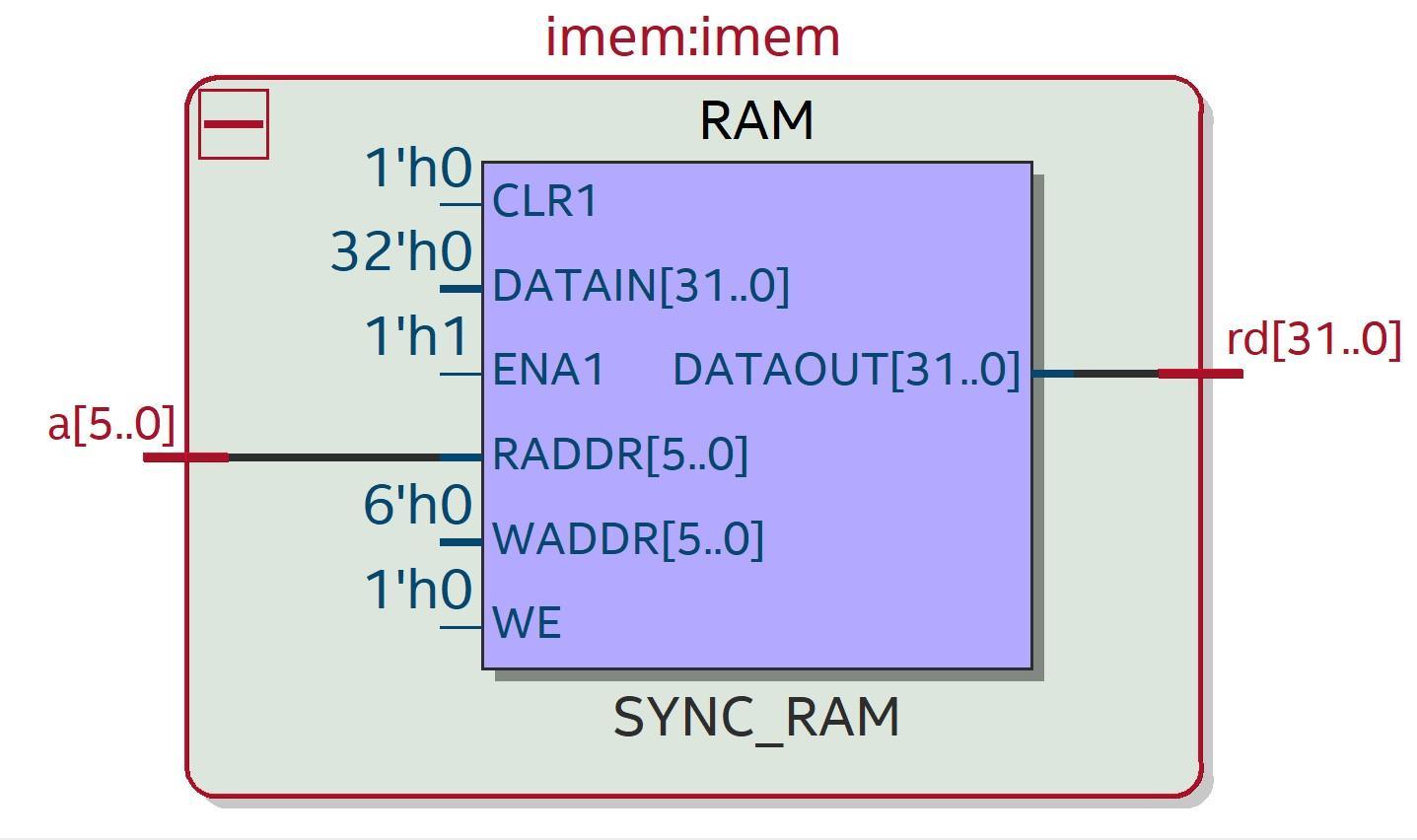
RTL view of Instruction Memory
4.MIPS
module mips(input clk, reset,
            output [31:0] pc,
            input [31:0] instr,
            output memwrite,
            output [31:0] aluout, writedata,
            input [31:0] readdata);

   wire memtoreg, branch,
   alusrc, regdst, regwrite, jump;
   wire [2:0] alucontrol;

   controller c(instr[31:26], instr[5:0], zero, memtoreg,
   memwrite, pcsrc, alusrc, regdst, regwrite, jump, alucontrol);

   datapath dp(clk, reset, memtoreg, pcsrc,alusrc, regdst, regwrite, jump,alucontrol,zero, pc, instr,aluout, writedata, readdata);

endmodule
Inputs :
- clk
- reset
- instr - current instruction being executed.
- 32 bit readdata - data read from the memory.
Outputs :
- 32 bit pc - current program counter.
- 32 bit aluout - result of ALU operation(i applicable).
- 32 bit writedata
- memwrite - control signal (discussed earlier).
The asm module instantiates two other modules, controller and datapath , which work together to execute instructions. Both these modules are discussed in detail in the upcoming sections.
Overall the asm module acts like a traffic signal, directing the flow of data and control signals between the datapath and controller modules to execute instructions and maintain the processor’s state.
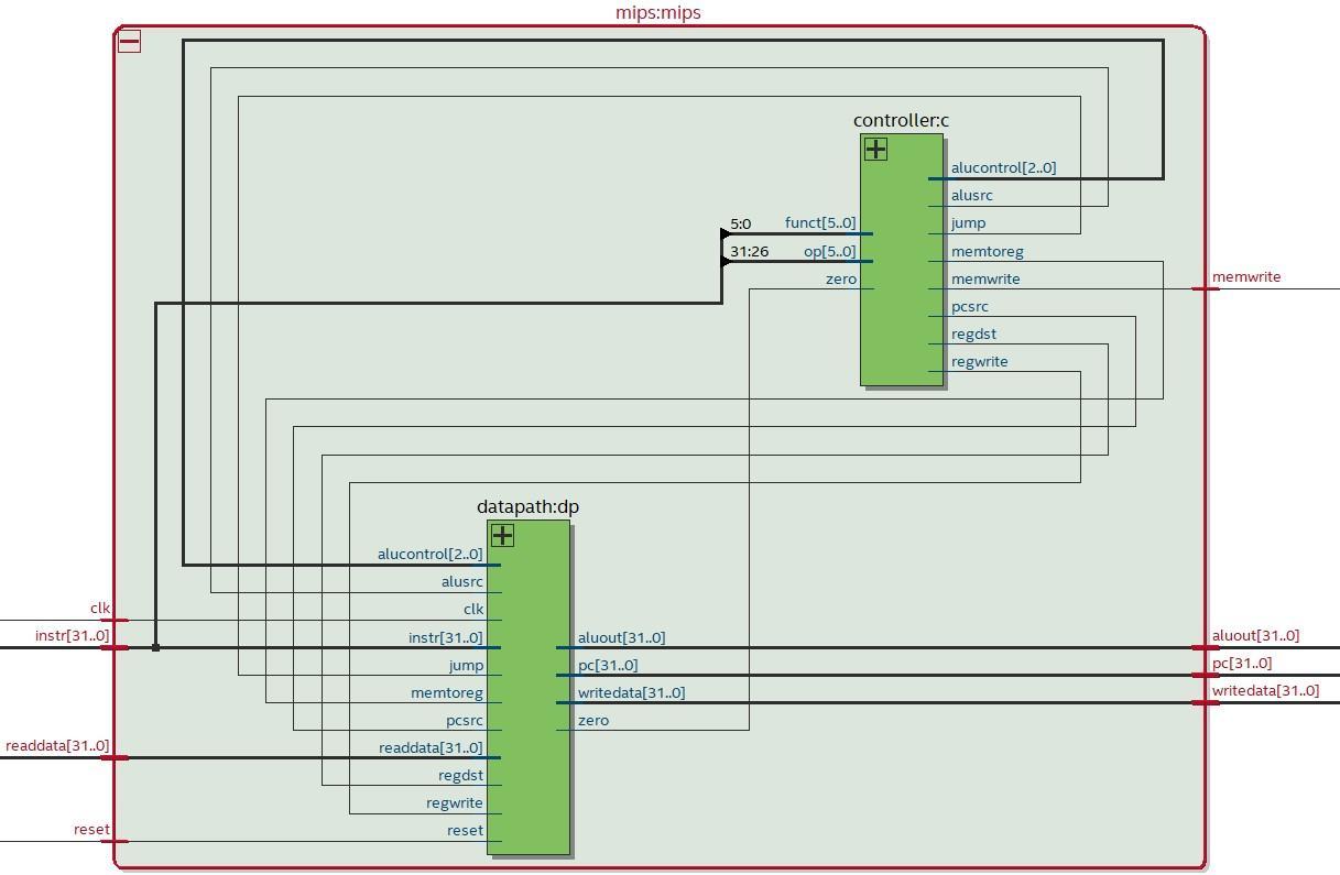
RTL view of MIPS module
5. Controller
module controller (input [5:0] op, funct,
                input zero,
                   output memtoreg, memwrite,
             output pcsrc, alusrc,
             output regdst, regwrite,
             output jump,
             output [2:0] alucontrol);

     wire [1:0] aluop;
     wire branch;

     maindec md (op, memtoreg, memwrite, branch,alusrc,   regdst, regwrite, jump,aluop);
     aludec ad (funct, aluop, alucontrol);

     assign pcsrc = branch & zero;
     endmodule
Inputs-
- 6 bit Opcode
- 6 bit funct
- Zero bit (for PCSrc)
Outputs-
7 control signals
memtoregmemwritepcsrcalusrcregdstregwritejump
3 bit alu control
Temporary Variables
- 2 bit AluOP
- Branch bit
Working
It acts as a top level module connecting the main decoder and alu decoder. It has some additional logic to make the PCSrc control signal by AND-ing the branch (intermediate) signal from the main decoder and the Zero from the ALU.
RTL View of Main Controller
6. Main Decoder
module maindec(input [5:0] op,
            output memtoreg, memwrite,
            output branch, alusrc,
            output regdst, regwrite,
            output jump,
            output [1:0] aluop);

     reg [8:0] controls;
     assign {regwrite, regdst, alusrc, branch, memwrite,  memtoreg, jump, aluop} = controls;

    always @ (*)
    case(op)
        6'b000000: controls <= 9'b110000010; //Rtype
        6'b100011: controls <= 9'b101001000; //LW
        6'b101011: controls <= 9'b001010000; //SW
        6'b000100: controls <= 9'b000100001; //BEQ
        6'b001000: controls <= 9'b101000000; //ADDI
        6'b000010: controls <= 9'b000000100; //J
        default: controls <= 9'bxxxxxxxxx; //???
    endcase
endmodule
Input :
6 Bit Opcode
Outputs :
memtoregmemwritebranchalusrcregdstregwritejump
(These 7 represent the 7 control signals which originate from the Control Unit and are explained in Theory section Table 1) 1. 2 Bit ALUOp
Temporary Variables
- 9 bit register control - It represents all the control signals together for easier assignment during the case statement.
Working
It is the main decoder which sets the control signals to 1s and 0s according to the opcode instruction. It uses a switch-case statement to decide what control to set inside a “always” procedural block.
Note:
always@(*)blocks are used to describe Combinational Logic, or Logic Gates.*sets the sensitivity list of the “always” to any values that can have an impact on a value(s) determined by thealways@(*)block.
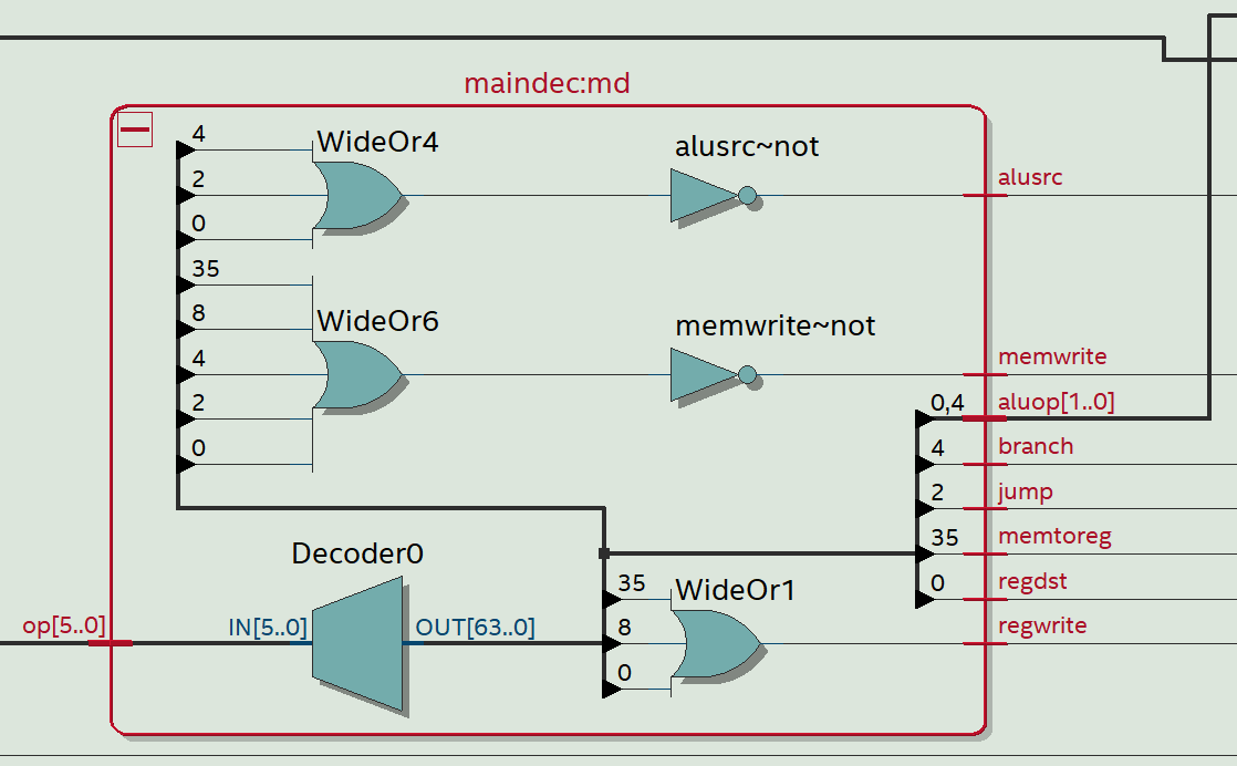 RTL View of Main Decoder
7. ALU Decoder
module aludec (input [5:0] funct,
               input [1:0] aluop,
         output reg [2:0] alucontrol);

   always @ (*)
        case (aluop)
            2'b00: alucontrol <= 3'b010; // add
            2'b01: alucontrol <= 3'b110; // sub
            default: case(funct) // RTYPE
                6'b100000: alucontrol <= 3'b010; // ADD
                6'b100010: alucontrol <= 3'b110; // SUB
                6'b100100: alucontrol <= 3'b000; // AND
                6'b100101: alucontrol <= 3'b001; // OR
                6'b101010: alucontrol <= 3'b111; // SLT
                default: alucontrol <= 3’bxxx; // ???
        endcase
endcase
endmodule
Inputs :
- 16 bit
funct(from 32 bit MIPS Instruction) - 2 bit
ALUOp(coming from Main decoder)
Output :
- 3 bit ALU control
Working
It decides what function the ALU will carry out. It works with a nested switch-case statement. First it checks the ALUop
- If
ALUOp= 1 -> ALU has to perform addition. (lw,sw) - If
ALUOp= 2 -> ALU has to perform subtraction. (beq) - If
ALUOp= 3 -> It depends on the 6 bit funct which will ADD, SUB, AND, OR, SLT (R-type)
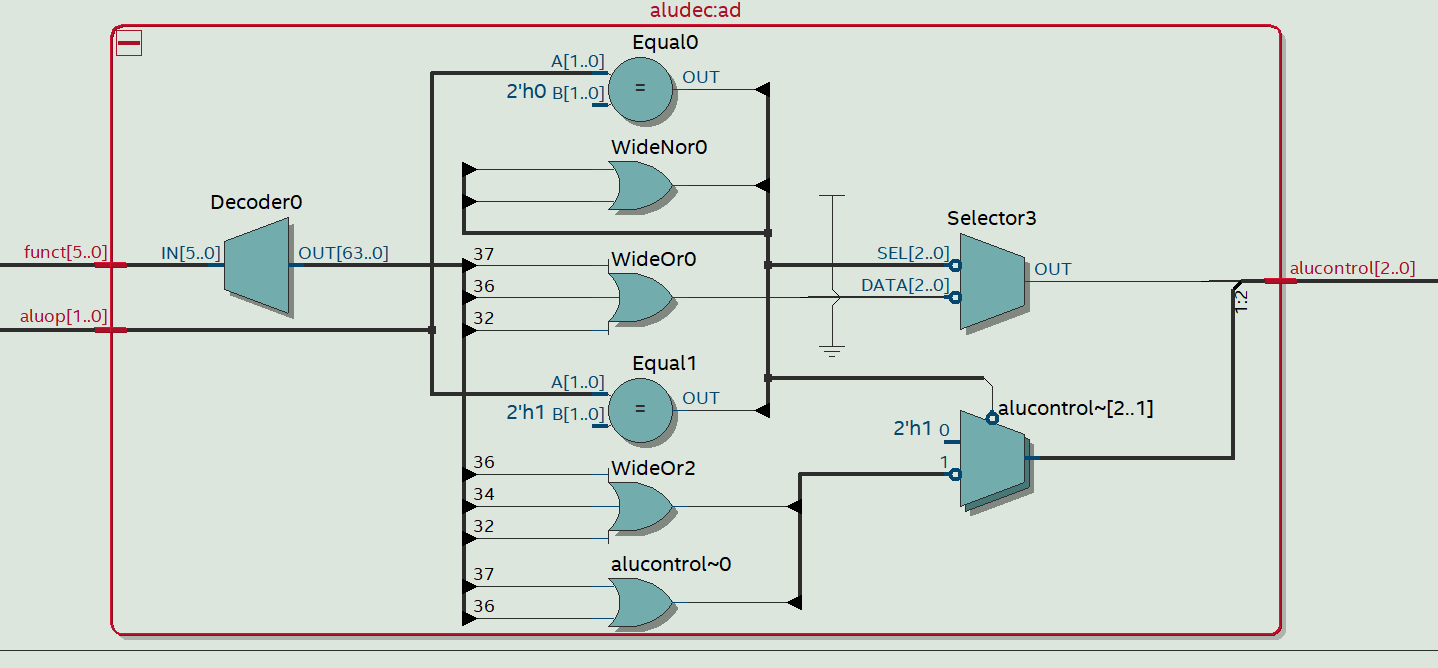 RTL View of ALU Decoder
8. Datapath
module datapath (input clk, reset,
    input memtoreg, pcsrc,
    input alusrc, regdst,
    input regwrite, jump,
    input [2:0] alucontrol,
    output zero,
    output [31:0] pc,
    input [31:0] instr,
    output [31:0] aluout, writedata,
    input [31:0] readdata);
    wire [4:0] writereg;
    wire [31:0] pcnext, pcnextbr, pcplus4, pcbranch;
    wire [31:0] signimm, signimmsh;
    wire [31:0] srca, srcb;
    wire [31:0] result;
// next PC logic
    flopr #(32) pcreg(clk, reset, pcnext, pc);
    adder pcadd1 (pc, 32b100, pcplus4);
    sl2 immsh(signimm, signimmsh);
    adder pcadd2(pcplus4, signimmsh, pcbranch);
    mux2 #(32) pcbrmux(pcplus4, pcbranch, pcsrc,pcnextbr);
    mux2 #(32) pcmux(pcnextbr, {pcplus4[31:28],
    instr[25:0], 2b00},jump, pcnext);
// register file logic
    regfile rf(clk, regwrite, instr[25:21],instr[20:16], writereg,result, srca, writedata);
    mux2 #(5) wrmux(instr[20:16], instr[15:11],
    regdst, writereg);
    mux2 #(32) resmux(aluout, readdata,
    memtoreg, result);
    signext se(instr[15:0], signimm);
// ALU logic
    mux2 #(32) srcbmux(writedata, signimm, alusrc,srcb); alu alu(srca, srcb, alucontrol,aluout, zero);
endmodule
Inputs :
- clk
- reset
(They are external inputs.) - memwrite
- regwrite
- regdst
- alusrc
- memtoreg
- pcsrc
- jump
(They are the control signals from the main decoder.) - 32 bit instr - output of the instruction memory.
- 32 bit readdata - output of the data memory.
- 3 bit alucontrol - output of the alu decoder.
Outputs :
- zero
- 32 bit pc
- 32 bit aluout
- 32 bit writedata
Working :
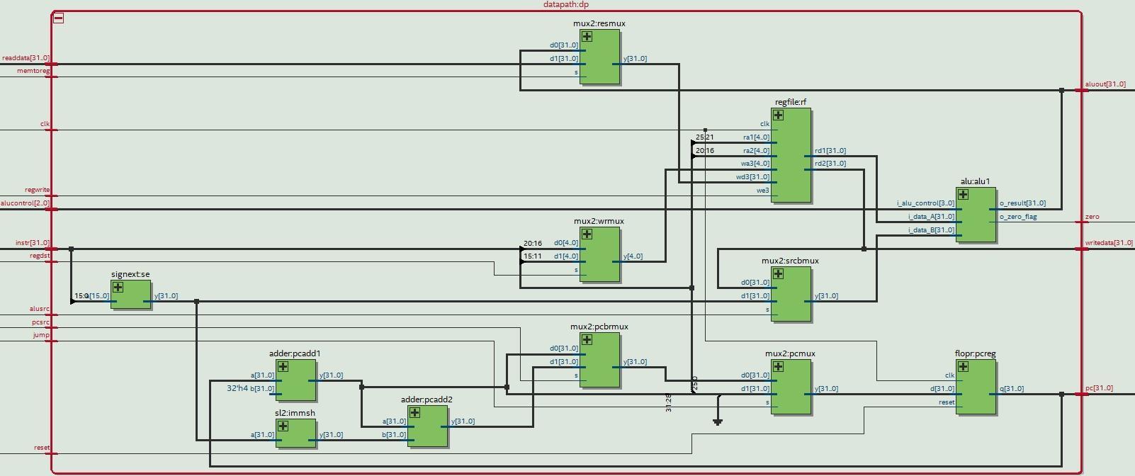
The datapath is separated into 3 sections:-
- next PC logic
The pseudocode for this section is-
{
always@(poseedge clk && poseedge reset)
    pc=pcnext;

    pcplus4=pc+4;
    signimm=signextend to 32 bits instr[15:0]
    signimmsh=shift left 2 of signimmsh
    pcbranch=pcplus4+signimmsh
    jump address= {pcplus4[31:28],instr[25:0], 2b00}

    if(pcsrc==0)
        pcnextbr=pcplus4;
    else
        pcnextbr=pcbranch;

    if(jump==0)
        pcnext=pcnextbr;
    else
        pcnext=jump address;
}- register file logic
The pseudocode for this section is-
{
if(regdst==0)
    writereg=instr[20:16];
else
    writereg=instr[15:11];
    if(memtoreg==0)
    result=aluout;
    else
    result=readdata;
    in registerfile {
    read register1=instr[25,21];
    read register2=instr[20:16];
    write register=writereg;
    write data=result;
          }
}- ALU In this section the ALU performs operations on ‘srca’(output of register file) and ‘srcb’ (depends on control signal alusrc) depending on the value of ‘alucontrol’.
RTL view of datapath
9. Three ported Register
module regfile (input clk,
                input we3,
                input [4:0] ra1, ra2, wa3,
                input [31:0] wd3,
                output [31:0] rd1, rd2);
                reg [31:0] rf[31:0];

    always @ (posedge clk)
    if (we3) rf[wa3] <= wd3;
        assign rd1 = (ra1 != 0) ? (rf[ra1]) : 0;
        assign rd2 = (ra2 != 0) ? (rf[ra2]): 0;
endmodule
Inputs :
Clksignal for third port- Read register 1
ra1 - Read register 2
ra2 - Write register
wa3 - Write data
we3
Outputs :
- Read data 1
rd1 - Read data 2
rd2
Temporary Variables :
- 32 element Array of 32 bit registers
Working :
Two ports read combinationally. Third port written on the rising edge of the clock. If any of the registers are ‘0’ it is hardwired to be 0 value by default.
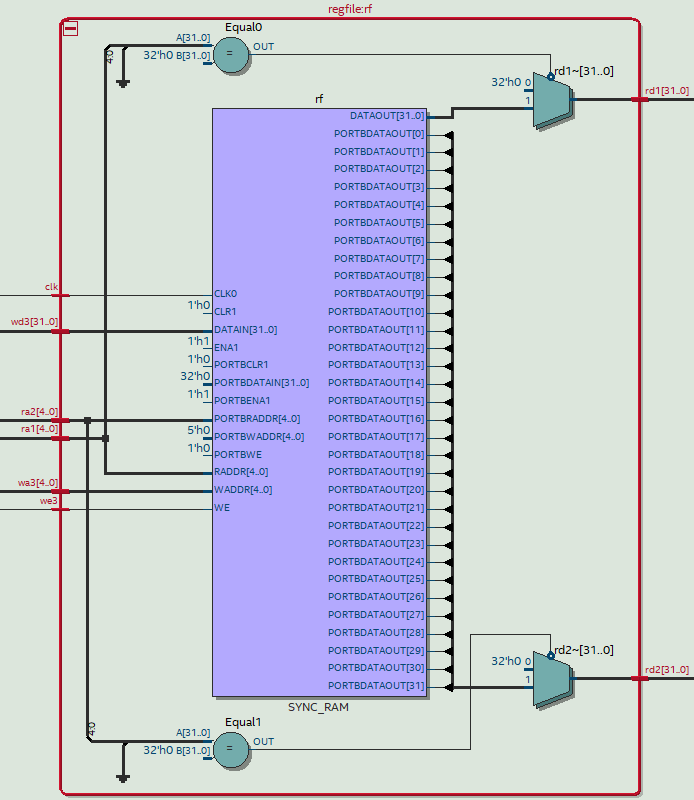 RTL View of Register File
10. Some Other Functional Units
These units were explained in previous modules. As such explanation and theory is not repeated and can be referred to from those modules.
1. ADDER MODULE
module adder (input [31:0] a, b,output [31:0] y); assign y=a + b;
endmodule
2. SHIFT LEFT BY 2 MODULE
module sl2 (input [31:0] a,
output [31:0] y);
assign y = {a[29:01], 2'b00};
endmodule
3. SIGN EXTENSION MODULE
module signext (input [15:0] a,output [31:0] y); assign y={{16{a[15]}}, a};
endmodule
First 16 bits of 32 bit Y are assigned the value of A[15] thus extending A by 16 bits.
4. D FLIP FLOP MODULE (with variable width)
module flopr # (parameter WIDTH = 8)(input clk, reset,input [WIDTH-1:0] d,output reg [WIDTH-1:0] q);
    always @ (posedge clk, posedge reset)
        if (reset) q<=0;
        else q <= d;
endmodule
5. 2 WAY MUX MODULE (with variable width)
module mux2 # (parameter WIDTH = 8)(input [WIDTH-1:0] d0, d1,input s,output [WIDTH-1:0] y);
assign y = s ? d1 : d0;
endmodule
6. 32 BIT ALU MODULE
module alu(i_data_A, i_data_B, i_alu_control,o_result,o_zero_flag);
    input [31:0] i_data_A; // A operand input [31:0] i_data_B; // B operand output reg [31:0] o_result; // ALU result input [3:0] i_alu_control; // Control signal
    output wire o_zero_flag; // Zero flag assign o_zero_flag = ~|o_result;
    always @(*) begin
    // Start initialization:
        casex(i_alu_control)
        4'b0010: // ADD
            begin
            o_result = i_data_A + i_data_B;
            end
        4'b0110: // SUB
            begin
            o_result = i_data_A - i_data_B;
            end
        4'b0000: // AND
            begin
            o_result = i_data_A & i_data_B;
            end
        4'b0001: // OR
            begin
            o_result = i_data_A | i_data_B;
            end
        4'b0111: // SLT
            begin
                o_result = i_data_A < i_data_B ? 32'h00000001: 32'h00000000;
            end
        4'b0011://XOR
            begin
                o_result=i_data_A^i_data_B;
            end
        4'b0100://NOR
            begin
                o_result=~(i_data_A | i_data_B);
            end
        default:
            begin
                o_result={32{1'bx}};  //x-state,(nor1,nor0)
            end
        endcase
    end
endmodule
6. How to Run Instructions
Great! Now we have our single cycle microprocessor ready but how do we run assembly code in it? The following steps explain that in detail. ( Since its a MIPS implementation of a 32 Bit Microprocessor we shall use MIPS code as the assembly code. )
Steps to run
- Write Down the MIPS code you want to execute.
- Your code should have an instance of the instruction you want to test.
- Make sure the set of instructions ends with a store word (sw) instruction. The output of this “store word” should be dependent on the instruction to be tested. (This will be used for checking if the instruction is executed correctly or not.)
- Convert the MIPS Code into machine code with the help of an online convertor.
- Save the machine code as “memfile.dat” in your preferred directory.
- Update the path (line 6) of “memfile.dat” in the imem module (Instruction Memory) of your Verilog code to the absolute path of the memfile.dat
- Change the test bench to check the following
- dataaddr- should contain the address of the last store word (X) in the last line of our machine code in memfile.dat
- writedata- should contain the data being written in memory (Y) in the last store word instruction.
- So, in the testbench make the change : (dataadr === X & writedata === Y )
- Save the module and compile your Verilog code.
- Run RTL Simulation.
- The transcript section should contain “Simulation succeeded” in the case of a correct implementation and matching dataaddr and writedata.
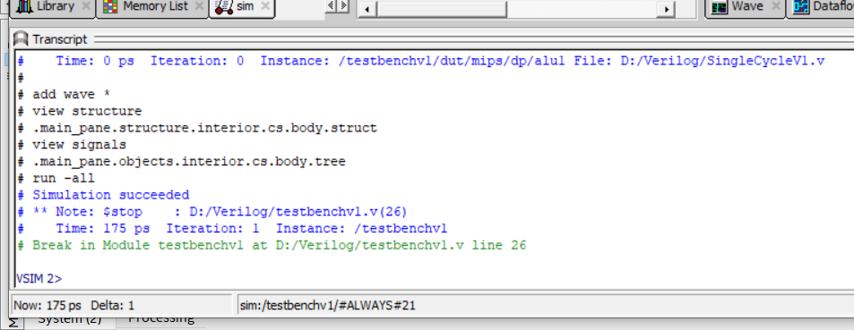
Fig. Sample transcript output
7. Test cases for Various Instructions
Now we will try to check if our microprocessor implements instructions properly.
1. add
addi $2, $0, 450 //initialise $2 =450
addi $3, $0, 550 //initialise $3 =550
add  $4, $2, $3  //$4=$2+$3 ,$4=450+550=1000
sw   $4, 20($0)  //write address 20 = 1000
Machine code
200201c2
20030226
00432020
ac040014
If the value at address location 20 is 1000,then the add instruction is working properly. The testbench to check the same is:
module testbenchv1;
    reg clk;
    reg reset;
    integer i;
    wire [31:0] writedata, dataadr;
    wire memwrite;

    // instantiate device to be tested
        top dut(clk, reset, writedata, dataadr, memwrite);
    // initialize test
    initial
        begin
            reset <= 1; # 22; reset <= 0;
        end

    // generate clock to sequence tests
    always
        begin
            clk <= 1; # 5; clk <= 0; # 5;
        end

    // check results
    always @ (negedge clk) begin
        if (memwrite) begin
        if (dataadr === 20 & writedata === 1000) begin
            $display ("Simulation succeeded");
            $stop;
        end
        else if (dataadr !== 80) begin
            $display ("Failed hehe %h and
            %h",writedata,dataadr);
            $stop;
        end
    end
    end
endmodule
2. sub
addi $2,$0, 550 //initialise $2 =550
addi $3,$0, 550 //initialise $3 =550
sub $4,$2, $3 //$4=$2+$3 , $4=550-550=0
sw $4, 50($0) //write address 50 = 0
Machine code :
20020226
20030226
00432022
ac040032
If the value at address location 50 is 0,then the sub instruction is working properly. The testbench to check the same is:
module testbenchv1;
    reg clk;
    reg reset;
    integer i;
    wire [31:0] writedata, dataadr;
    wire memwrite;
    // instantiate device to be tested
    top dut(clk, reset, writedata, dataadr, memwrite);
    // initialize test
        initial
            begin
                reset <= 1; # 22; reset <= 0;
            end
    // generate clock to sequence tests
        always
            begin
                clk <= 1; # 5; clk <= 0; # 5;
            end
    //check results
    always @ (negedge clk)
    begin
        if (memwrite) begin
            if (dataadr === 50 & writedata === 0) begin
                $display ("Simulation succeeded");
                $stop;
            end
            else if (dataadr !== 80) begin
                $display ("Failed hehe %h and
                %h",writedata,dataadr);
                $stop;
            end
        end
    end
 endmodule
3. sw
addi $2,$0,25 //initialise $2 =25
sw $2, 30($0) //write address 30 = 25
Machine code :
20020019
ac02001e
If the value at address location 30 is 25,the sw instruction is working properly. The testbench to check the same is:
module testbenchv1;
    reg clk;
    reg reset;
    integer i;
    wire [31:0] writedata, dataadr;
    wire memwrite;
    // instantiate device to be tested
    top dut(clk, reset, writedata, dataadr, memwrite);
    // initialize test
    initial
    begin
    reset <= 1; # 22; reset <= 0;
    end
    // generate clock to sequence tests
    always
    begin
    clk <= 1; # 5; clk <= 0; # 5;
    end
    // check results
    always @ (negedge clk)
    begin
        if (memwrite) begin
            if (dataadr === 30 & writedata === 25) begin
                $display ("Simulation succeeded");
                $stop;
            end
            else if (dataadr !== 80) begin
                $display ("Failed hehe %h and
                %h",writedata,dataadr);
                $stop;
            end
        end
    end
endmodule
4. lw
addi $2,$0,100 //initialise $2 =100
sw $2,30($0) //write address 30 = 100
lw $3,30($0) //$3=[30] = 100
sw $3,20($0) //write address 20 = 100
Machine code
20020064
ac02001e
8c03001e
ac030014
If the value at address location 20 is 100, then lw instruction is working properly. The testbench to check the same is:\
module testbenchv1;
    reg clk;
    reg reset;
    integer i;
    wire [31:0] writedata, dataadr;
    wire memwrite;
    // instantiate device to be tested
    top dut(clk, reset, writedata, dataadr, memwrite);
    // initialize test
    initial
        begin
        reset <= 1; # 22; reset <= 0;
        end
    // generate clock to sequence tests
    always
        begin
        clk <= 1; # 5; clk <= 0; # 5;
        end
    // check results
    always @ (negedge clk)
        begin
        if (memwrite) begin
            if (dataadr === 20 & writedata === 100) begin
            $display ("Simulation succeeded");
            $stop;
            end
            else if (dataadr !== 30) begin
                $display ("Failed hehe %h and
                %h",writedata,dataadr);
                $stop;
            end
        end
    end
endmodule
5. beq
main:
addi $2,$0,20 //initialise $2 =20
addi $3,$0,30 //initialise $3 =30
addi $5,$0,0 //initialise $5 =0
beq $5,$0,end //if val($5)==val($0) branch to ‘end’ add $5,$2,$3 //$5=$2+$3
end:
sw $5, 20($0) //write address 20 = 0
Machine code:
20020014
2003001e
20050000
10a00002
00432820
ac050014
If the value at address location 20 is 0,then the beq instruction is executed properly. The testbench for the same is:
module testbenchv1;
    reg clk;
    reg reset;
    integer i;
    wire [31:0] writedata, dataadr;
    wire memwrite;
// instantiate device to be tested
    top dut (clk, reset, writedata, dataadr, memwrite);
// initialize test
initial
    begin
        reset <= 1; # 22; reset <= 0;
    end
// generate clock to sequence tests
always
     begin
         clk <= 1; # 5; clk <= 0; # 5;
     end
// check results
    always @ (negedge clk)
    begin
        if (memwrite) begin
            if (dataadr === 20 & writedata === 0) begin
                $display ("Simulation succeeded");
                $stop;
            end else if (dataadr !== 80) begin
                $display ("Failed hehe %h and
                %h",writedata,dataadr);
                $stop;
            end
        end
    end
endmodule
8. References
- "Computer Organization and Design: The Hardware/Software Interface" by David Patterson and John Hennessy
- “Digital design and Computer architecture” by David Money Harris & Sarah L. Harris.
- “Digital Logic and Computer Design ”by M. Morris Mano.
- “Verilog HDL: A Guide to Digital Design and Synthesis ” by Samir Palnitkar.
