Introduction To Registers
Visit Code Repository
Registers
A register is a collection of flip-flops that are edge triggered. Registers capture and store data based on a trigger- either a rising or falling edge. Registers are crucial for CPUs as they serve as temporary data storage elements. To code for a register using behavioural modelling in Verilog, it is expected of us to mimic the behaviour of a register using a variable such that it is assigned a value and stores it until the next edge triggering. We shall discuss how to implement a register using D flip-flops as well.
The reg datatype in Verilog is used to declare variables which model data storage elements, they store the value assigned to them and can represent either combinational or sequential logic.
To design a simple 4-bit register in Verilog in which only 1 operation – read or write is allowed at a time, we need to declare:1. A reg variable with the required number of bits (4 in this case) to act as our register.2. A read/write signal as input (one or multiple depending on whether the question permits more than one operation to be performed at a time).3. A reset signal which enables us to reset the value in the register to 0- it can be active high or low.4. Input ports: write_data for the data to be written, read_address and write_address (both are not necessary here since we write to only 1 register but we'll see them in register files).
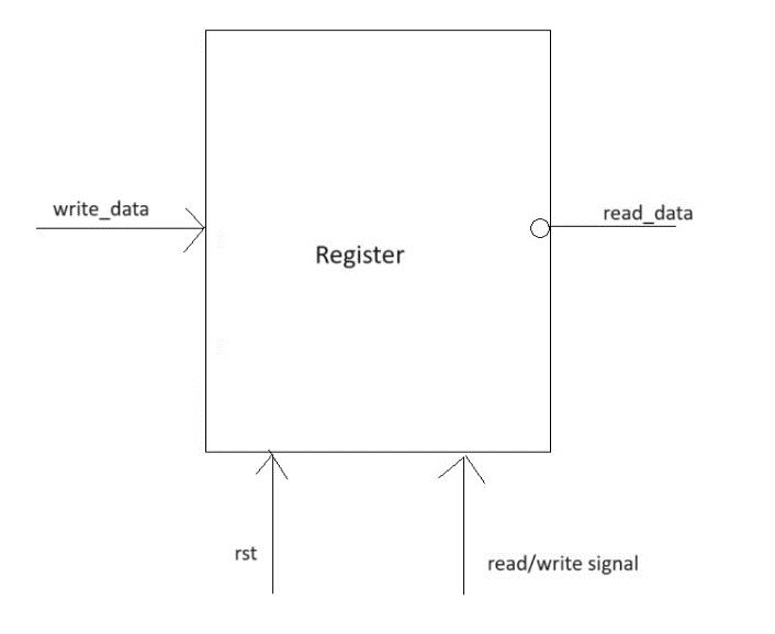
5. Output port: read_data, write to it when the read/write signal is high and read its value when the read/write signal is low.
module register(input clk, rst, rw,
                input [3:0] write_data,
                output [3:0] read_data);

    reg [3:0] block;
    always@(posedge clk) begin
        if(!rst)   block <= 0;
        else begin
            if(rw==1) block <= write_data;
            else read_data <= block;
        end
    end
endmodule
Since we have written our read logic in the else block, even if the rw signal is any value other than 0 or 1 at the beginning we just read the register displaying its contents, which is ‘x’ initially. This is to avoid unintentionally writing a value, giving read operation a higher priority over write. You can initialize the block reg to 0 too (it can depend on the question).
If we have a register with multiple read and write ports, the question will mention certain specifications for e.g. reads can occur parallelly but not writes. To demonstrate how to go about coding for such a question, let us see an example of a 4-bit register with 1 read ports and 2 write ports. A read and write operation cannot occur simultaneously but we can have 2 such writes and every time we write to the register, we alternately use either of the write ports. Initially, when we perform a write operation, we write into the register with write_data_1, the next time with write_data_2, etc.
module reg_wr(input clk,
              input rst,
              input rw,
              input[15:0] data1, data2,
              output reg [15:0] read);
    // perform writ1 & writ2 alternatively
    reg [15:0] block;
    reg track=0;
    always@(posedge clk) begin
        if(rst==0) begin // reset is active low
            read <= 0;
        end
        else if(rw==0) begin // write
            if(track==0) begin
                block <= data1;
                track <= 1;
            end
            else begin
                block <= data2;
                track <= 0;
            end
        end
        else begin // read
            read <= block;
        end
    end
endmodule
To design a register using flip-flops, let’s consider the first example wherein we had a 4-bit register with one read and write port. We instantiate four D flip-flops and assign the incoming input as input to the flip-flops if the rw signal is high, else we assign the contents of the flip-flop to the output variable. Note that in case of the write operation, the output variable reflects the previously read/stored value.
module dflfl(output reg op, input ip, input clk);
    always @(posedge clk) begin
        op <= ip;
    end
endmodule

module four_bit_reg(output reg [3:0] out, input [3:0] ip, input clk, input rw);
    reg [3:0]intermed;
    reg [3:0]temp;

    dflfl g1(temp[3], rw ? ip[3]:temp[3], clk);
    dflfl g2(temp[2], rw ? ip[2]:temp[2], clk);
    dflfl g3(temp[1], rw ? ip[1]:temp[1], clk);
    dflfl g4(temp[0], rw ? ip[0]:temp[0], clk);

    always @(*) begin
        if(rw==1'b1) intermed <= temp; // storing previous value in intermed
    end

    always @(posedge clk) begin
        if(rw==1'b1) out <= intermed; // if a write occurs then previously read value is displayed
        else out <= temp; // else in case of a read
    end
endmodule
When we instantiate the D flip-flops, we check whether the rw signal is high i.e. whether a write is occurring to pass the input to it. Since we cannot mix case and if else statements with our combinational block i.e. we cannot instantiate the dffs conditionally (Verilog does not support this), the dffs will therefore be instantiated at every rising edge transition and so for a read operation, we pass it dummy data which would be the previously written (currently stored) value.
Register Files
Register Files contain an array of registers. Hence there is a need for read and write address inputs to ascertain which register to read from or write data into.
Ports are input and output signals. When a question mentions that the register has to have multiple read ports or multiple write ports- this means that there are several read_address, write_address and write_data ports- we can perform more than 1 operation at the same time on different registers within the register file. There are several cases to consider in such questions- if a question permits multiple writes at the same time, you need to think of the possibility of more than one operation attempting to write to the same register, or if a read and write can occur together, you need to think of the possibility of an operation attempting to read from and another attempting to write to the same register. So assigning priorities is important. More than one read operation occurring simultaneously won’t create a problem.
Let’s look at the code for a register file with 8 registers capable of storing 8-bit data each. It has 2 read ports and 1 write port. Two reads are permitted simultaneously, however only read or write is allowed at a time.
module reg_file(input clk, rst,
                input [1:0]r1r2w,
                input[2:0] port1,
                input[2:0] port2,
                input [2:0] port3,
                input [7:0] data,
                output reg [7:0] read1, read2);

    reg [WIDTH-1:0] block[WIDTH-1:0];
    // 2 read ports, 1 write port
    always@(posedge clk) begin
    // r1r2w- 0: write case
    // r1r2w- 1: read1 case
    // r1r2w- 2: read2 case
    // r1r2w- 3: read1 & read2 case
        if(rst==0) begin
            read1 <= 0;
            read2 <= 0;
        end
        else if(r1r2w == 0) begin // write
            block[port1] <= data;
        end
        else if(r1r2w == 1) begin
            read1 <= block[port2];
        end
        else if(r1r2w == 2) begin
            read2 <= block[port3];
        end
        else begin
            read1 <= block[port2];
            read2 <= block[port3];
        end
    end
endmodule
We declare a r1r2w signal because we are permitted to perform two reads but a read and write cannot occur simultaneously. Besides the ports, we declare an array of eight eight-bit registers in Verilog in this format: reg [x:0] block [y:0] where you declare the number of bits of each register before the variable name ‘block’ and the number of array elements i.e. registers after block.
Here's a pictorial representation of the register file: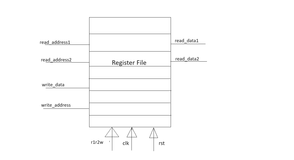
If we are permitted to perform multiple write operations, then we must assign priorities to the write ports. We can do this by structuring our if else blocks in a favourable manner.
Let’s assume that we have eight eight-bit registers contained in a register file that has 1 read port and 2 write ports. Similar to the last example, we cannot have a read and write operation at once but we can perform both write operations simultaneously. In case two writes try to access the same register, give priority to write_data_1.
module reg_file(input clk, rst,
                input [1:0] rw1w2,
                input [2:0] write_add_1,
                input [2:0] write_add_2,
                input [2:0] read_add,
                input [7:0] write_data_1,
                input [7:0] write_data_2,
                output reg [7:0] read_data);

    parameter WIDTH=8;
    reg [WIDTH-1:0] block[WIDTH-1:0];

    always@(posedge clk) begin
    // rw1w2- 0: read case
    // rw1w2- 1: write1 case
    // rw1w2- 2: write2 case
    // rw1w2- 3: write1 & write2 case
        if(rst==0) begin
            read_data <= 0;
        end
        else if(rw1w2 == 0) begin // read
            read_data <= block[read_add];
        end
        else if(rw1w2 == 1) begin // write1
            block[write_add_1] <= write_data_1;
        end
        else if(rw1w2 == 2) begin // write2
            block[write_add_2] <= write_data_2;
        end
        else begin
            if (write_add_1 == write_add_2)
                block[write_add_1] <= write_data_1;
            else begin
                block[write_add_1] <= write_data_1;
                block[write_add_2] <= write_data_2;
            end
        end
    end
endmodule
Q: Can you take the previous example and modify it such that the register file now has 2 read ports and 2 write ports and any pair of operations can occur simultaneously? Let the read operation be of higher priority when a read and write occur simultaneously, and if two operations attempt to write to the same register, let the one with the lower serial number e.g. write_data_1 over write_data_2 be of higher priority.
Shift Registers
Shift registers are a cascade of flip-flops used to store values which are passed on to the consecutive register at every edge triggering. They are used for temporary data storage, data transfer and data manipulation. Here is an example of a SISO (Serial In, Serial Out) type shift register:
Assuming that the ffs are initialized to store a value of 0. Data can be serially shifted to the left or right, in this example we shift to the right. 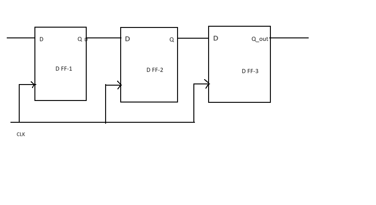
| CLK Transition | D | Q1 | Q2 | Q_out |
|---|---|---|---|---|
| ↑ | 1 | 1 | 0 | 0 |
| ↑ | 1 | 1 | 1 | 0 |
| ↑ | 0 | 0 | 1 | 1 |
| ↑ | 0 | 0 | 0 | 1 |
| ↑ | 1 | 1 | 0 | 0 |
| ↑ | 0 | 0 | 1 | 0 |
This example shown above is that of a SISO shift register wherein there is only 1 (serial) input and 1 output each such that the data is stored and shifted bit by bit sequentially either leftwards or rightwards.
Other types of shift registers include:1. SIPO: Serial In, Parallel Out (One input, outputs Qi where i=1,2,..,n for each of the n flipflops)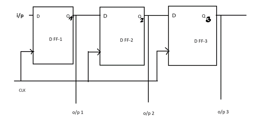
| CLK Transition | D | Q1 | Q2 | Q_out |
|---|---|---|---|---|
| ↑ | 1 | 1 | 0 | 0 |
| ↑ | 1 | 1 | 1 | 0 |
| ↑ | 0 | 0 | 1 | 1 |
| ↑ | 0 | 0 | 0 | 1 |
| ↑ | 1 | 1 | 0 | 0 |
| ↑ | 0 | 0 | 1 | 0 |
2.PISO: Parallel In, Serial Out (Multiple inputs fed separately to each ff, one output Q_out)
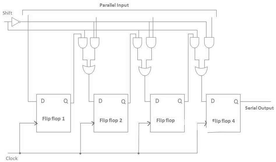 [Image Credit: GeeksForGeeks](https://www.geeksforgeeks.org/piso-shift-register/)
 3. PIPO: Parallel In, Parallel Out (Separate inputs for each ff, separate outputs at each ff)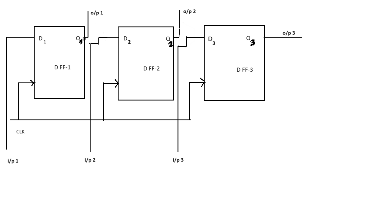
| CLK Transition | D1 | D2 | D3 | Q1 | Q2 | Q3 |
|---|---|---|---|---|---|---|
| ↑ | 1 | 0 | 1 | 1 | 0 | 1 |
| ↑ | 1 | 0 | 0 | 1 | 0 | 0 |
| ↑ | 0 | 0 | 1 | 0 | 0 | 1 |
| ↑ | 0 | 0 | 0 | 0 | 0 | 0 |
| ↑ | 1 | 1 | 1 | 1 | 1 | 1 |
| ↑ | 0 | 1 | 0 | 0 | 1 | 0 |
Let’s look at the design of a 4-bit shift register (SISO) in Verilog:
module shift_reg(input clk, en, in, output reg out);
    reg [3:0] sreg;
    integer i;

    always@(posedge clk) begin
        if(en) begin
            for(i=0; i<3; i++) begin
                sreg[i+1] <= sreg[i];
                sreg[0] <= in;
            end
            out <= sreg[15];
        end
    end
endmodule
When the EN signal is active, the shift register operates according to SISO logic; however, when the EN signal is inactive, no shifting or alteration occurs.
If we were to implement a 4-bit shift register (SISO) with D flip-flops (hierarchical modelling), it would look like this:
module dflfl(output reg op, input ip, input clk);
    always @(posedge clk) begin
        op <= ip;
    end
endmodule

module siso(output reg [3:0] out,
            input ip,
            input clk,en);
   reg [3:0] temp;

   dflfl g1(out[3], en ? ip:out[3], clk);
   dflfl g2(out[2], en ? out[3]:out[2], clk);
   dflfl g3(out[1], en ? out[2]:out[1], clk);
   dflfl g4(out[0], en ? out[1]:out[0], clk);

 endmodule
This is an example of a shift right SISO shift register wherein the input gets serially shifted to the right at every positive edge triggering. The combinational block involves instantiation of four D flip-flops and applying the serial shifting logic by passing the input to the MSB flip-flop. The inputs to the other flip-flops are the outputs of the flip-flops preceding them. If the enable signal is low, we freeze the current values and we don’t make any changes.
Q: Attempt to design a bidirectional shift register in Verilog.
We need to have two modes- shift left and shift right, and so we have an additional input control signal.
Try it out and see if you can implement it in code.
Q. Attempt to design a 4-bit SIPO shift register in Verilog. What changes would you have to make to the SISO code and what additional input and output signals would you have to include?
Some useful short notes
1. A note on parameterization: The code that we write for n-bit registers is limited for registers which are strictly n-bits. In order to write code and design registers that are more reusable, that can accommodate an arbitrary number of bits for each instantiation, we can utilize instantiation parameters. We can pass the required value of the parameter at the time of instantiation and we can also specify a default value.
module register #(parameter WIDTH=4) (
    input clk, rst, rw,
    input [WIDTH-1:0] write_data,
    output [WIDTH-1:0] read_data);
    reg [WIDTH-1:0] block;

    always@(posedge clk) begin
        if(!rst)   block <= 0;
        else begin
            if(rw==1) block <= write_data;
            else read_data <= block;
        end
    end
endmodule
The syntax for parametrizing a module is:
module module_name #(parameter PARAMETER_NAME =default_value) (declare input and output signals)
